Part four of a series on how to build your own computer from scratch, based around the Z80 CPU.
In this series, Robin builds a Z80 computer from scratch. Catch up with parts 1–3.
In the last episode, we made a USB serial EEPROM programmer so we can put data onto our ROM. In this episode, we will add some basic IO and learn some Z80 assembler so we can write our first program!
Schematic
How It Works: Z80 IO
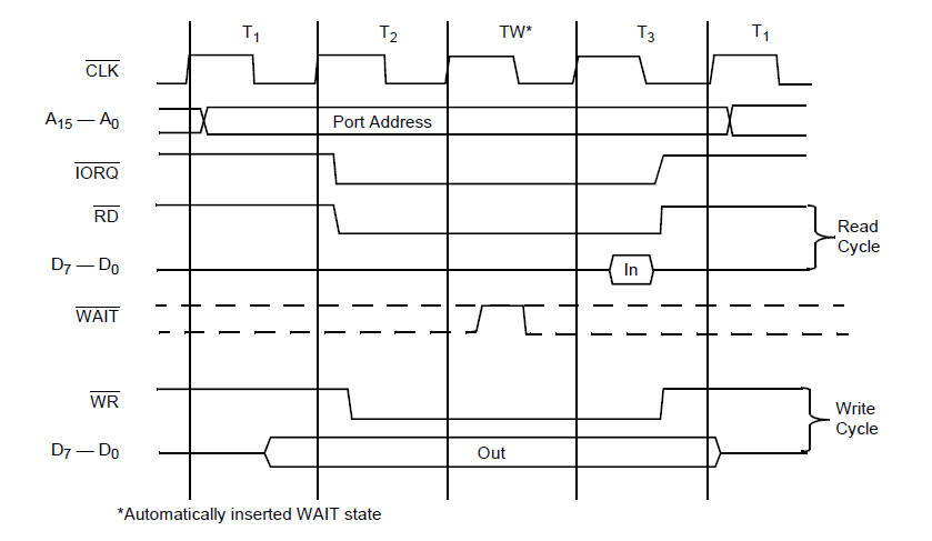
In the second episode in this series, we looked at how the Z80 interacts with memory using the different signals RD, WR, and MREQ. IO devices interact with the Z80 in an almost identical way, with a few differences. When accessing memory, the address pins point to a memory location, and since the address range is 16 bits, you can access up to 65,536 different locations. When accessing IO, only half of the address range is used (A0–A7) and the values of A8–A15 contain the value of register A. Therefore, a single IO instruction can only access one of 256 IO devices instead of the full 16-bit range. However, if needed, register A could have a number assigned to it before an IO access is made, and this would allow for up to 65,536 devices (this, however, is rarely seen in designs since it takes up computing time).
Below is the timing diagram for IO device access using the Z80. The top half (above the dotted line) shows a read cycle, while the bottom half shows the write cycle. Unlike the memory cycle, neither MREQ is used and there is no additional wait state (TW).
Extract from the Z80 datasheet
Now that we understand how the Z80 reads and writes to an IO device, it’s time to look at the circuitry. The first task is to decode the Z80 address so that, depending on the value of the address, a specific device can be selected with its own chip select line. To do this, we use a 4515, which is a demultiplexer that converts a 4-bit input into a 16-wire output. The 4515 also has two other inputs, EL and EN, which stand for “enable latch” and “enable,” respectively. For our project, we don’t care about the EN signal, so we tie that to VCC, but we connect EN to IORQ. When IORQ goes low, this also brings EN low, which enables the multiplexer. However, remember that the 4515 has inverted outputs, so if, for example, the first output is selected, it will be a logical 0 instead of a logical 1. We use this chip because most chip select lines are inverted (active low), and thus help to reduce external circuitry.
Now that we know how the 4515 IC works, which address pins do we connect the 4-bit input to? It would seem to make sense if we connect these to the Z80’s A0–A3 pins, but instead, we are going to connect them to the Z80’s A4–A7. Why would we do this? The answer lies in practicality and usability! First, no computer has 256 IO devices, and our computer will struggle to use 16 IO devices, so the 4515 is useful in this scenario for IO decoding. Secondly, by using the upper four bits as the IO device selector, we can use the lower four bits as commands and circuit signals. Imagine if we have an IO device that can do 16 different things; instead of connecting 16 IO lines to that device, we can instead use one IO line to access it and use the lower 4 address bits to tell it to do one of 16 different commands. The picture below shows how an IO address is split up into IO devices and 4 command bits.
With this system, our IO devices have the following addresses:
- Switches – IO Address 0x00
- LEDs – IO Address 0x10
Z80 Assembler: Your First Program
Now that our Z80 has some basic IO, it’s time to learn some basic Z80 assembler and how to make our first program! While Z80 assembler instructions themselves are usually simple, there are many of them, and they all do different things. To keep things easy, we will look at the most basic instructions relevant to this tutorial as well as the internal structure of the Z80.
The Z80 has internal registers which are either used to hold temporary variables or be used as pointers that point to a memory location. The most commonly used register is A, mainly because it is one of the main registers used with the ALU that performs all mathematical and many logical functions. Other registers available include B, C, D, E, H, and L. The Z80, despite being an 8-bit CPU, has some 16-bit instructions, which use 8-bit pair registers. These register pairs are BC, DE, and HL. Other useful registers also include the flag register (F, which holds information such as carry, negative, and overflow), and the index registers I, X, and Y. However, these are not important in this tutorial and therefore will not be covered.
Approximate internal structure of Z80. Image courtesy Wikipedia.
Many operations done by the Z80 only operate on registers (while some operate on memory locations), which is why your code will spend a lot of its transferring data between the registers and the RAM. But, fortunately for us, in this tutorial, we do not require RAM, as we will only be using one variable which we will hold in register A. So what will our first program do? Our program’s objective will be to read the states of the tactile switches and then display this state on the LEDs. This means that we need to make the Z80 read the tactile switch IO device and then send this state to the LED IO device.
To write assembler programs, we will use a free software called tniASM, which is incredibly powerful and has many features, including multi-pass design, conditional assembly, local label mechanism, source and binary inclusion, and nestable block comments. While it is unclear if redistribution is allowed, this project comes with tniASM and a bat file to make it easy to compile assembler programs with it. Your first task is to unzip the project files, locate the folder assembler, open the folder source, and load the file main.asm in either notepad or your favourite text editor (Notepad ++ works best here). If all goes well, you should see the following:
The first code that tniASM looks at is “cpu Z80,” which tells it that it is compiling code for the Z80 processor. The next line is “org 0x0000,” which tells it where our program will sit in the memory (remember, our ROM goes from 0x0000 to 0x00FF). These lines are not code that the Z80 will see, but configuration data for the assembler.
Line 13 is the first instruction that the Z80 will execute and has the label main. The instruction here is in a, (0) and this causes the Z80 to select IO device 0 (the tactile switches), read the databus, and put the value seen on the databus into register A. The second line is the second instruction that the Z80 will execute, which is “out (0x10), a.” When this is executed, the Z80 will select the IO device 0x10 (the LEDs), and write the value in register A to it. The last instruction is a goto instruction called jump (“jp”) and this will jump to the label main. It is important to know that the Z80 itself does not do jump to label and only does either absolute jumps to memory addresses or relative jumps. The label “main” is seen by the compiler (tniASM) and converted into a memory location. In this example, main is the very first instruction, which means its memory address will be 0x0000. Therefore, jp main is actually jp 0x0000.
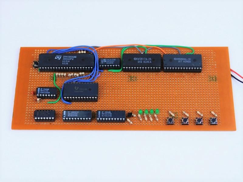
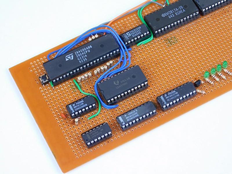
Construction
A project like this should be constructed using a method that either allows the saving of ICs and/or saving of other components. However, construction methods like solderless breadboards are not the best, because they have real speed limits when going beyond 4MHz (which we will do in the future); so methods such as using stripboards are advised. You could use a different PCB, but due to the fact that we upgrade this machine each episode, it is best to not use such a permanent technique.
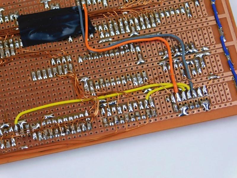
Most of the wiring for this project is on the underside and uses copper magnetic wire, which has a fantastic property — solderable enamel. Bare copper wires cannot be used as shown in this project, because they would easily touch other wires and metal connections, which would result in a short. You can use normal wires with plastic sleeves, but they are usually bulky and quickly result in a shortage of wiring space. You can use enameled copper wire, but getting the enamel off can be very tricky, which is why I used solderable enamel wire. The coating itself is an insulator, but when in contact with molten solder, it melts and forms a nice electrical connection, which makes it ideal in situations where there will be large bundles of wires (as seen below).
Related Articles